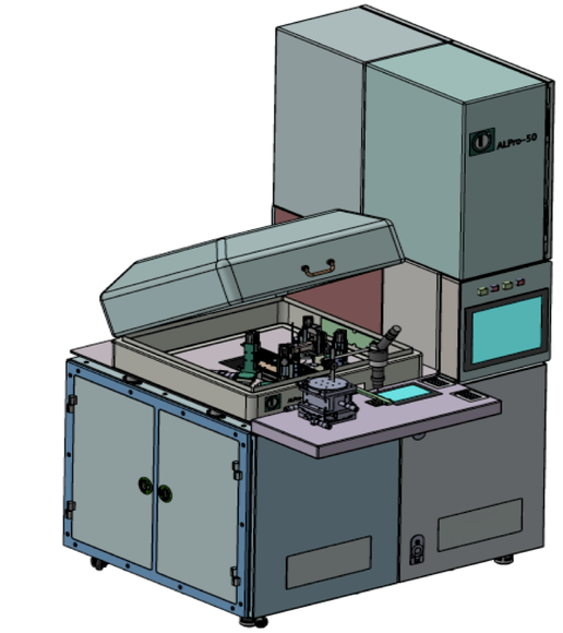
Figure Caption: A 3D drawing of the ALPro-50 metrology tool developed by ALP.
Semiconductor industry is the engine of economic, environmental and social development in the world. Many applications from machine learning to artificial intelligence and robotics all depend on the availability of faster running integrated circuits or chips, with higher computing power and data storage capability. Integrated circuits manufacturers have been shrinking the size of the transistor for the last five decades, increasing the number of transistors integrated in a chip from about 2500 in 1970’s to over 10 billion today. Miniaturization brings the cost of the integrated circuits down, and at the same time improves its performance with higher speeds and more functionality per chip. Today’s transistors are nanometer size devices that are 1000 times smaller than the typical thickness of human hair.
Miniaturization of devices comes with many challenges. One of these challenges is the precise measurement of the electrical properties of the nanometer thick layers employed in the transistor structure. These properties include the carrier concentration and mobility depth profiles, both of which are important to know since they eventually determine the performance of the transistor. The existing methods used to measure such properties, such as spreading resistance profiling and scanning spreading resistance microscopy, are becoming limited in their resolution as the film thicknesses shrink.
I am Co-Founder/CEO of Active Layer Parametrics (ALP), a Silicon Valley startup developing a novel metrology technique for the semiconductor industry, (www.alpinc.net). Our company developed ALPro technology, which has the ability to provide depth profiles of all electrical properties through thin semiconductor layers at a depth resolution better than 0.3 nanometers, approaching atomic level (see Figure 1). This is the best resolution offered by any technology available today. We developed ALPro technology under a Small Business Innovation Research program funded by the National Science Foundation. The ALPro profiling technique reduces the thickness of the film to be characterized at a specific test site on a wafer sample by a highly controllable approach and keeps measuring the properties of the remaining layer. From these differential measurements, a depth profile of the electrical property may then be derived.
Two important developments in the commercialization of this novel technology have been the acceptance of our company ALP as a portfolio company of Silicon Catalyst, a Silicon Valley incubator focused on semiconductor solution startups (www.siliconcatalyst.com), and the sale of the first commercial ALPro-50 tool to EAG laboratories, the largest global technical services company in the world (www.eag.com/news-post/eag-first-alp-metrology-tool/). Ability to measure the electrical properties of nano-layers employed in advanced semiconductor devices at atomic level resolution is expected to provide valuable information to process/device development engineers at semiconductor equipment vendors, research organizations and IC manufacturers to accelerate their development cycles.
Dr. Bulent Basol
Bulent Basol is the Co-Founder/CEO of Active Layer Parametrics (ALP), a Silicon Valley startup developing a novel metrology technique for the semiconductor industry. Basol started several high tech companies throughout his career. He developed multiple thin film photovoltaic technologies including an electroplated cadmium telluride technology that yielded the most efficient modules of its time; an ink printing based copper indium gallium selenide technology that demonstrated the first efficient devices by such techniques, and the first efficient ultra-light weight CIS solar cell on a polyimide foil, which won an innovation award from NASA. As a founder of SoloPower he developed a roll-to-roll manufacturing method for flexible solar module fabrication. In the area of semiconductors Basol developed novel deposition/polishing technologies for integrated circuits industry. Bulent received his B.S. degree in Electrical Engineering at Bogazici University (1973) and Ph.D. from UCLA. He has over 100 publications and 167 issued US patents and several international patents.